


Research Finder
Find by Keyword
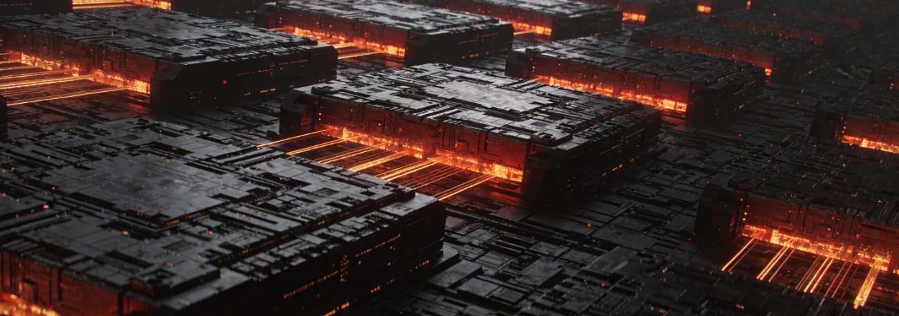
Will Musk’s $25 Billion Terafab Gamble Redefine the Global Chip Supply?
Exploring the joint venture between Tesla, SpaceX, and xAI aiming to deliver one terawatt of AI compute through integrated 2nm manufacturing.
3/24/2026
Key Highlights
- Terafab aims to produce 100 billion to 200 billion AI chips annually (some news reports have it at millions, but the math works out to billions) using a 2nm process node.
- The facility was architected to integrate logic, memory, and advanced packaging under a single roof; later, Musk acknowledged that several sites will likely be used.
- Musk’s joint venture faces significant hurdles regarding process IP and specialized equipment lead times.
- Industry analysts estimate total capital requirements could reach $45 billion, exceeding initial guidance.
The News
Elon Musk announced Terafab, a $25 billion joint venture between Tesla, SpaceX, and xAI located with a toehold in Travis County, Texas with an enormous facility elsewhere. The facility aims to deliver one terawatt of compute annually to support autonomous systems and orbital AI. No specific manufacturing partner or equipment orders from ASML were confirmed during the presentation. Find out more by following Elon Musk on X.
Analyst Take
We have reached a stage where betting against Elon Musk feels like a bit of a fool's errand. He has successfully disrupted aerospace, forced the global automotive industry to embrace electrification, and proved us wrong about internal chip design. Tesla’s custom silicon for Full Self-Driving worked and stayed competitive against established giants. However, the announcement of Terafab represents a move into a fundamentally different industrial arena. We reckon that designing a chip is a bit like writing a brilliant play; manufacturing that chip is more akin to building and operating the entire theater network. The risks are different, the capital is heavier, and the margin for error is razor-thin.
What Was Announced
The Terafab initiative is architected to function as a production hub for logic, memory, and advanced packaging. It aims to deliver approximately one terawatt of annual compute capacity; this translates to a volume of roughly 100 billion to 200 billion AI chips every year. Some media reports have this at 100-200 million, but the math would indicate billions. The facility is designed to occupy the existing Tesla campus in eastern Travis County, Texas. Musk followed up after the announcement that several other facilities may be required as well. Financially, the project is architected around an initial $20 billion to $25 billion investment; however, market estimates suggest the true cost for a 2 nanometer facility of this scale may reach $45 billion. The technical specification targets the 2 nanometer process node, which represents the current bleeding edge of semiconductor physics. This joint venture between Tesla, SpaceX, and xAI aims to consolidate the entire compute supply chain under a single corporate umbrella. The architecture is designed to support a recursive design loop, where mask creation and testing occur on-site to reduce iteration cycles to as little as a company-claimed <7 day pace.
The heavy tilt toward orbital AI (roughly 80 % of output) introduces deep-space realities that dwarf terrestrial 2 nm challenges. The project includes custom D3 chips explicitly engineered to run hotter (minimizing radiator mass), survive total ionizing dose and single-event radiation effects, and operate in thermal vacuum conditions at terawatt scale. Starship’s payload revolution, measured in millions of tons to orbit annually, unlocks in-orbit servicing or even partial fab testing concepts that no earthly foundry can replicate. At the same time it creates fresh vulnerabilities: ITAR controls on radiation-hardened silicon and constellation-level cyber-physical security. This is no longer just “more chips”; it is a closed-loop Earth-to-orbit compute ecosystem the traditional supply chain simply cannot touch.
We see a massive gap between the ambition of this presentation and the practical realities of the semiconductor industry. To manufacture at 2 nanometers, a firm requires a proven process flow. Currently, only TSMC, Samsung, and Intel possess this, and they do not typically share their recipes. We might see a partnership with IBM Research, similar to the Rapidus model in Japan, but no such deal was mentioned. Without a partner, Tesla would have to develop a 2nm process from scratch. That is a Herculean task. Manufacturing is a different beast.
The equipment bottleneck is equally concerning. A 2nm fab requires multiple High-NA EUV lithography systems from ASML. These machines cost hundreds of millions of dollars and have waitlists that span years. We have not seen any confirmed orders from Tesla in the ASML backlog yet. The clock for a fab does not start when a press release is issued; it starts when the equipment slots are secured. Furthermore, a facility like Terafab requires thousands of specialized engineers. McKinsey analysis suggests that the United States faces a shortage of up to 90,000 fab workers by 2030. Recruiting this talent while competing with Intel and TSMC will be a spot of bother for Musk’s team.
Another unmentioned but existential hurdle is the staggering energy and resource demand. Musk has confirmed that Terafab at full scale will require over 10 GW of continuous power, that is the equivalent of several large nuclear plants. Other requirements will be thousands of acres and enormous volumes of ultra-pure water for fabrication and cooling. In drought-prone Texas this has the potential to trigger bruising ERCOT grid battles, water-rights litigation, and multi-year environmental permitting. Yet the same vertical integration that defines the project offers an escape hatch: co-locating Tesla Megapack storage and solar generation (or even evaluating small modular reactors) could create the world’s first energy-sovereign fab. Turning this apparent weakness into a structural opex advantage would give Terafab a differentiator few legacy foundries can match, provided the permitting clock does not swallow the timeline. In Texas he has a better chance than elsewhere, but this is still going to be a stretch.
The strategic logic for Terafab is sound even if the execution remains a question. We see a global foundry capacity crunch that will likely persist through 2030. Bain and Company research suggests that total global compute requirements could reach 200 gigawatts by the end of the decade. If you believe in the volume projections for the Optimus humanoid robot, the internal demand for chips at Tesla alone could exceed what any external foundry can provide. Musk is identifying a genuine strategic vulnerability. He wants to own the means of production to avoid being held hostage by third-party lead times. This makes sense.
However, we must look at the financial strain. Tesla is already guiding for significant capital expenditures in 2026. A $40 billion fab project would likely require raising additional capital. We also remember the Dojo supercomputer project. It was hyped as a revolutionary step, then the team was disbanded, and then it was restarted. This inconsistency makes us cautious. Musk’s pattern is to announce aggressively and deliver eventually, often with revised scopes and higher costs. For a car, that works. For a 2nm fab, the physics of the process node are less forgiving. We want to see the team. We want to see the orders. Until then, we remain skeptical of the timeline.
Looking Ahead
Based on what we are observing, the Terafab announcement reflects a broader trend toward the vertical integration of the entire AI stack. As compute becomes the most valuable commodity in the global economy, the most ambitious firms are no longer content to outsource the fabrication of their core IP. We reckon that Musk is attempting to build a "sovereign compute" model that bypasses the traditional foundry system entirely. When you look at the market as a whole, the announcement signals that the era of fabless design dominance may be reaching its limit for the largest AI players.
The key trend that we are going to be looking out for is how Tesla navigates the process IP gap. Our perspective is that Terafab will likely evolve into an advanced packaging and technology center rather than a standalone 2nm foundry. We might see them license IBM's nanosheet technology or perhaps strike a deep manufacturing partnership with Intel Foundry. Going forward, we are going to be closely monitoring how the company performs on its recruitment of senior semiconductor manufacturing leadership. Hiring a few designers is easy; staffing a world-class fab is a different challenge.
What could ultimately separate Terafab from a high-risk copycat is xAI’s potential to weaponize Grok itself against the manufacturing learning curve. The on-site recursive loop Musk described (with daily iterations in the research fab) could be turbocharged by AI-driven yield prediction, real-time anomaly detection, and process-flow simulation that bypasses decades of human heuristics. Musk explicitly flagged exploration of “non-traditional computing.” This opens the door to photonics integration, analog/mixed-signal designs, or aggressive 3D stacking that leap past pure-CMOS 2 nm power walls. Paired with a probable IBM nanosheet license or Intel Foundry co-development, the result could be less a 2 nm foundry and more a physics-breaking advantage no legacy player possesses.
When you look at the competitive landscape, this move puts pressure on TSMC and Samsung to offer more favorable terms to their "anchor" customers. Musk has previously used this kind of bold announcement to pressure industry players in AI and automotive to move faster in support of his goals. HyperFRAME will be tracking how the company does in securing equipment slots from ASML in future quarters. If those orders do not materialize by the end of 2026, the 2028-2030 production window will likely shift. We see this as a high-risk, high-reward play for Musk. Success would change the industry. Failure would be costly, but.

Steven Dickens | CEO HyperFRAME Research
Regarded as a luminary at the intersection of technology and business transformation, Steven Dickens is the CEO and Principal Analyst at HyperFRAME Research.
Ranked consistently among the Top 10 Analysts by AR Insights and a contributor to Forbes, Steven's expert perspectives are sought after by tier one media outlets such as The Wall Street Journal and CNBC, and he is a regular on TV networks including the Schwab Network and Bloomberg.
Share
Stephen Sopko | Analyst-in-Residence – Semiconductors & Deep Tech
Stephen Sopko is an Analyst-in-Residence specializing in semiconductors and the deep technologies powering today’s innovation ecosystem. With decades of executive experience spanning Fortune 100, government, and startups, he provides actionable insights by connecting market trends and cutting-edge technologies to business outcomes.
Stephen’s expertise in analyzing the entire buyer’s journey, from technology acquisition to implementation, was refined during his tenure as co-founder and COO of Palisade Compliance, where he helped Fortune 500 clients optimize technology investments. His ability to identify opportunities at the intersection of semiconductors, emerging technologies, and enterprise needs makes him a sought-after advisor to stakeholders navigating complex decisions.