


Research Finder
Find by Keyword
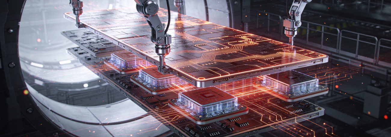
Can NEXX Acquisition Reshape Applied's Advanced Packaging Lead?
NEXX deal positions Applied for fine-pitch I/O wiring on panel substrates as AI workloads push package complexity beyond wafer scale
05/11/2026
Key Highlights
- Applied Materials announced a definitive agreement to acquire ASMPT Limited's NEXX business, designed to broaden Applied's panel-level advanced packaging portfolio.
- NEXX brings panel-level electrochemical deposition (ECD) technology, complementing Applied's wide array of existing systems in digital lithography, PVD, CVD, etch, and eBeam metrology and inspection.
- The acquisition aims to enable larger AI accelerator packages built on substrates as large as 510 by 515 millimeters, well beyond the limits of 300mm silicon wafers.
- The transaction is expected to close within the next several months and requires no regulatory approvals, with the NEXX team continuing to operate from Billerica, Massachusetts within Applied's Semiconductor Products Group.
- We observe this deal is less about "packaging" in the legacy sense and more about Applied positioning to industrialize a fundamentally different manufacturing form factor for AI compute.
The News
Applied Materials announced a definitive agreement with ASMPT Limited to acquire its NEXX business, a supplier of large-area advanced packaging deposition equipment for the semiconductor industry. The combination broadens Applied's portfolio of panel-level advanced packaging technologies in support of larger-body AI accelerators. These advanced packages are built up from chiplet-based designs integrating GPUs, high-bandwidth memory (HBM) stacks, and input-output (I/O) chips in a single package. NEXX's panel-level electrochemical deposition (ECD) technology aims to enable co-optimized solutions for fine-pitch I/O wiring, accelerating advanced packaging roadmaps for AI chipmakers and systems companies. The transaction is expected to close within the next several months and requires no regulatory approvals, with NEXX joining Applied's Semiconductor Products Group following close. (Applied Materials press release).
Analyst Take
The semantics of "packaging" in semiconductors have quietly become one of the most consequential (and poorly understood by outsiders) definitional debates in the industry. Applied Materials' acquisition of NEXX from ASMPT lands directly inside that debate.
In simple terms, traditional packaging is a mature, outsourced back-end service. Chipmakers dice finished wafers into individual dies, then send them to specialized assembly and test houses (OSATs) around the world that compete mostly on labor cost and throughput. These firms protect the die, add basic electrical connections (often via wire bonding or flip-chip), and encase everything in plastic or ceramic. It is a commodity step available in many places with relatively low margins.
Advanced packaging is something fundamentally different. It integrates multiple chiplets, high-bandwidth memory stacks, interposers, and fine-pitch wiring into a single high-performance unit — often while still at wafer or panel scale. The processes involved (sub-micron lithography, hybrid bonding, precision deposition, and metrology) now resemble front-end wafer fabrication in complexity, precision, and strategic importance. For AI accelerators, this step has moved from a back-end afterthought to a front-end-equivalent process that directly determines performance, power efficiency, yield, and overall economics. Applied itself frames advanced packaging as an increasingly important enabler of energy-efficient performance at both the chip and system level, a framing we think is directionally correct and arguably understates how central these processes have become to AI compute economics.
From our vantage point at HyperFRAME, having been in conversation with experts across the industry, we observe that what we still call "packaging" today bears almost no resemblance to the wirebonded, leadframe-mounted devices that defined the term for forty years. With this in mind, we see the real story not as 'Applied is buying a deposition company.' We see it as the industry quietly accepting that round wafers may very well no longer be the best manufacturing primitive for AI compute. That is a much bigger deal than the transaction itself.
What Was Announced
Applied has entered into a definitive agreement with ASMPT Limited to absorb its NEXX business, which specializes in large-area panel deposition equipment for advanced packaging. The deal would extend Applied's already broad panel-level toolkit, which spans: digital lithography, physical vapor deposition (PVD), chemical vapor deposition (CVD), etch, and eBeam metrology and inspection. Panel plating, by Applied's own description, has been an area in which the company did not previously hold a position, making the NEXX deal a deliberate fill of an identified gap rather than incremental capability stacking. NEXX's contribution centers on panel-level electrochemical deposition (ECD), the process used to plate copper into fine-pitch wiring channels that route signals between chiplets, HBM stacks, and I/O dies. NEXX brings what Applied characterizes as a large installed base of panel ECD tools across the world's advanced substrate factories, giving the combined entity an immediate production footprint rather than a clean-sheet market entry. To put the form-factor shift into perspective, the industry is migrating from 300-millimeter silicon wafers to rectangular panels measuring 510 by 515 millimeters or larger, dramatically increasing the available real estate for AI package design. This matters because "packaging" itself now encompasses several distinct disciplines, each with its own materials science, metrology requirements, and yield economics. The legacy definition (dicing, wirebonding, encapsulation) sits at one end. Wafer-level packaging (WLP) and fan-out wafer-level packaging (FOWLP) extend interconnect beyond the die while still anchored to round substrates. Then 2.5D interposer-based assembly, 3D die stacking with through-silicon vias, hybrid bonding for direct copper-to-copper interfaces, and now panel-level integration each represent a distinct manufacturing discipline. The company announced that NEXX will be incorporated into Applied's Semiconductor Products Group following close, continuing operations from its Billerica, Massachusetts base under President Jarek Pisera's existing team.
Market Analysis
The competitive context is more nuanced than a typical tools acquisition. Lam Research, Applied, and ASML have spent years competing primarily on front-end process tools. Now, the boundary between front-end and back-end is dissolving as chiplet integration becomes a yield-determining step. Multiple industry analysts and experts have a consensus that advanced packaging has shifted. It should no longer be thought of as simply a commoditized back-end activity, historically dominated by outsourced semiconductor assembly and test (OSAT) firms competing on labor cost, to a strategic differentiator that the major players are moving first to capture. Players failing to integrate advanced packaging into their offerings facing the risk of commoditization themselves. The competitive landscape around panel-level processing is more textured than a simple Applied-versus-everyone framing. Lam Research is Applied's most direct electrochemical deposition competitor, with its SABRE 3D electrofill family on the wafer side and a dedicated panel-level wet processing platform that scales beyond traditional wafer formats, putting Lam in essentially the same fight Applied is now fortifying with NEXX. Tokyo Electron commands the coater/developer market and operates a LITHIUS Pro AP platform engineered for advanced packaging, although TEL's panel-level posture remains less aggressive than Lam's, with most of its packaging tools still anchored to wafer formats. ASML's relevance to advanced packaging shifted in late 2025 when it shipped its first dedicated packaging lithography product, the Twinscan XT:260 i-line scanner, designed for CoWoS, fan-out, and hybrid bonding interconnects rather than panel substrates specifically. That move suggests ASML is targeting the front-end-adjacent layer of advanced packaging rather than the full panel manufacturing flow. BE Semiconductor is a case worth flagging carefully because it is not primarily an Applied competitor but a strategic partner. Applied took a 9 percent stake in BESI in April 2025, becoming its largest shareholder, and the two companies jointly developed the Kinex die-to-wafer hybrid bonding system. Reuters reported in March 2026 that BESI had received takeover approaches with Lam Research and Applied among potential acquirers, an outcome that would reshape the hybrid bonding competitive map regardless of how it resolves.
The NEXX acquisition slots directly into Applied's broader high-velocity innovation strategy anchored by the EPIC Center in Silicon Valley, on track to open this year as the largest collaborative R&D facility for chip equipment in the world. By bringing NEXX's panel ECD capability under the same roof as PVD, CVD, lithography, etch, and inspection systems, Applied is positioning the EPIC Center to function as a co-development hub for the full panel-level process flow rather than a sequence of bilateral handoffs. For TSMC, Intel, Samsung, SK Hynix, Micron, and the systems companies designing custom AI silicon, that integrated toolset is designed to compress development cycles for next-generation packages. ASMPT's decision to divest NEXX is informative on its own terms. The company appears to be focusing capital on its core back-end equipment franchise rather than competing with Applied's deposition scale, suggesting a strategic clarification about where each firm sees defensible economics in the panel era.
Looking Ahead
Based on what we are observing, the next eighteen months will determine whether panel-level packaging becomes a mainstream production format or remains a specialized capability reserved for the largest AI accelerator designs. Three things we will be tracking. First, whether OSATs and foundries adopt 510 by 515 mm panel formats at production scale, or whether competing form factors emerge from Japanese and Korean equipment vendors. Second, whether Applied's EPIC Center co-innovation model, once operational, produces measurable cycle-time compression for AI chipmakers compared to traditional sequential development. Third, whether the regulatory-free closing of the NEXX deal sets a template for further consolidation in the panel-level equipment space. The economics of AI compute are being rewritten at the package level, not just the transistor level. That is where our attention sits.

Stephen Sopko | Analyst-in-Residence – Semiconductors & Deep Tech
Stephen Sopko is an Analyst-in-Residence specializing in semiconductors and the deep technologies powering today’s innovation ecosystem. With decades of executive experience spanning Fortune 100, government, and startups, he provides actionable insights by connecting market trends and cutting-edge technologies to business outcomes.
Stephen’s expertise in analyzing the entire buyer’s journey, from technology acquisition to implementation, was refined during his tenure as co-founder and COO of Palisade Compliance, where he helped Fortune 500 clients optimize technology investments. His ability to identify opportunities at the intersection of semiconductors, emerging technologies, and enterprise needs makes him a sought-after advisor to stakeholders navigating complex decisions.